
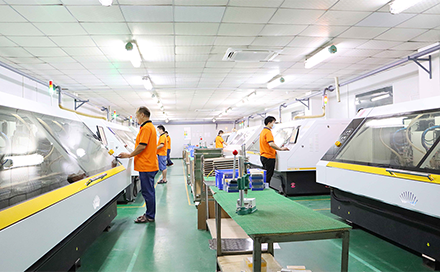
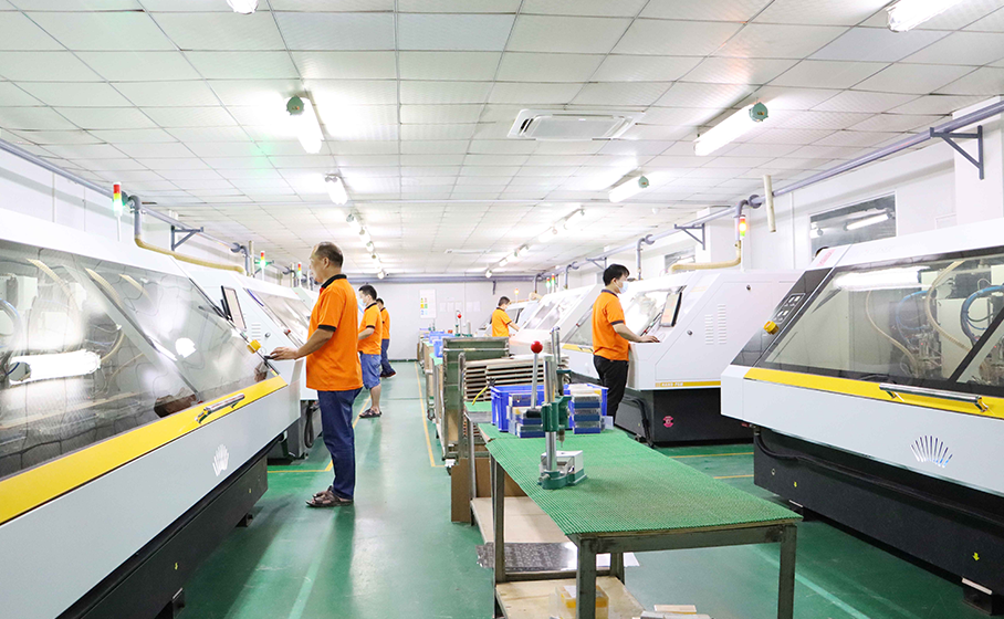
Before mass production of PCB circuit boards, it is generally necessary for PCB circuit board manufacturers to conduct sampling first, in order to make a small number of samples to test the quality of the products, and to some extent, to avoid risks for future large-scale production. So, what is the sampling process for PCB board manufacturers?
Step 1: Verify the data
Before production, the circuit board manufacturer will verify the board making data provided by the customer, including the size of the board, process requirements, and product quantity. The next step of production will only proceed after reaching an agreement with the customer.
Step 2: Material cutting
According to the customer's board making information, cut small pieces of production boards on the boards that meet the requirements. Specific operation: large plate material → cutting according to MI requirements → cutting the plate → cutting the corner/grinding the edge → discharging the plate.
Step 3: Drilling
Drill the required hole diameter at the corresponding position on the PCB board. Large plate material → Cutting according to MI requirements → Curing → Fillet/edge grinding → Plate discharge.
Step 4: Copper sinking
A thin layer of copper is deposited chemically on the insulating hole. Specific operations: rough grinding → hanging the board → automatic copper sinking line → lowering the board → soaking in 1% dilute H2SO4 → thickening the copper.
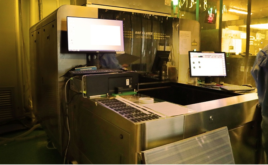
Step 5: Graph transfer
Transfer the images from the production film to the board. Specific operation: hemp board → film pressing → standing → alignment → exposure → standing → development → inspection.
Step 6: Graphic Plating
Electroplate a copper layer with the required thickness and a gold nickel or tin layer with the required thickness on the exposed copper sheet or hole wall of the circuit pattern. Specific operations: upper plate → degreasing → secondary water washing → micro corrosion → water washing → acid washing → copper plating → water washing → acid soaking → tin plating → water washing → lower plate.
Step 7: Remove the film
Remove the anti electroplating coating layer with NaOH solution and expose the non line copper layer.
Step 8: Etching
Remove non circuit parts with chemical reagent copper.
Step 9: Green Oil
Transfer the graphics of the green film onto the board, mainly to protect the circuit and prevent soldering of parts with tin on the circuit.
Step 10: Characters
Print recognizable characters on the PCB board. Specific operation: After the green oil is finally cured, cool and stand still, adjust the screen, print characters, and finally cure.
Step 11: Gilded Fingers
Apply a nickel/gold layer of the required thickness on the plug finger to enhance its hardness and wear resistance.
Step 12: Forming
Punch the shape required by the customer using a mold or CNC gong machine.
Step 13: Testing
It is not easy to detect functional defects caused by open circuits, short circuits, etc. through visual inspection, and can be tested using a flying needle tester.
The above is the process of PCB board factory sampling, hoping to be helpful to you!
Popular Blog Posts

PCB Manufacturing & Assembly Service
 File Upload


Our Newsletter
PCB
Assembly
Capabilities
About
Contact
- Building 18, Shayi North Yongfa Science Park, Xinhe
Road, Shajing Street, Bao'an District, Shenzhen, China
- Email:[email protected]
- Skype:
- WhatsApp:8613528898321
- Tel:+86 13528898321(David Wang )
- Fax:4007752975
Payment Methods:

Delivery Services

Verified by
