

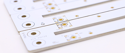
Ceramic PCB is a thermal conductive organic ceramic circuit board with thermal conductivity of 9-20W/m.k prepared at a temperature below 250°C using thermally conductive ceramic powder and organic adhesive,ceramic PCB types by material including alumina PCB, Aluminum nitride ceramic PCB,Copper clad ceramic PCB, Zirconia ceramic base PCB.
| Ceramic Substrate Material | Thermal Conductivity |
| Aluminum Nitride | 150 – 180 W/mK |
| Aluminum Oxide | 18-36 W/mK |
| Beryllium Oxide | 184-300 W/mK |
| Boron Nitride | 15 – 600 W/mK |
| Silicon Carbide | 70-210 W/mK |
Development Background of Ceramic PCB

With the development of electronic technology, the highly integrated circuit board has become an inevitable trend. The highly integrated package module requires a good heat dissipation system, while the disadvantage of the traditional FR-4 and CEM-3 is in TC (thermal conductivity), which restricts electronic technology development. In recent years, the LED industry’s rapid development has also put forward higher requirements for the TC indicators of its load-bearing circuit boards. In high-power LED lighting, circuit substrates are often prepared from materials with good heat dissipation properties such as metals and ceramics. The thermal conductivity of high thermal conductivity aluminum substrates is generally 1-4W/M. K and the thermal conductivity of ceramic substrates depend on the method of preparation. Different from the material formula, it can reach about 220W/M. K.
Four Processes of Ceramic PCB Material
Traditional ceramic substrate manufacturing methods can be divided into four types: HTCC, LTCC, DBC, and DPC.
1.The HTCC (high temperature co-fired) preparation method requires a temperature above 1300°C, but due to the choice of the electrode, the preparation cost is quite expensive.
2.The LTCC (low temperature co-firing) requires a calcination process of about 850°C, but circuit precision is poor, and the thermal conductivity is low.
3.The DBC requires formingan alloy between the copper foil and the ceramic, and the calcination temperature needs to be strictly controlled within the temperature range of 1065-1085°C. Because the DBC requires the thickness of the copper foil, generally, it cannot be less than 150-300 microns. Therefore, the wire width to depth ratio of such ceramic circuit boards is limited.
4.The preparation methods of DPC include vacuum coating, wet coating, exposure and development, etching, and other process links, so the price of its products is relatively high. In addition, in terms of shape processing, DPC 1800 ceramic fiber board plates need to be laser cut. Traditional drilling and milling machines and punching machines cannot accurately process them, so the bonding force and line width are more precise.
Alumina Ceramic Substrate

Aluminum Nitride Ceramic PCB
The alumina ceramic substrate has high mechanical strength, good insulation, and light resistance. It has been widely used in multilayer wiring ceramic substrates, electronic packaging, and high-density packaging substrates.
1.The Crystal Structure, Classification, and Performance of Alumina Ceramic Substrate
Alumina has many homogenous crystals, such as α-Al2o3, β-Al2o3, γ-Al2o3, etc. Among them, α-Al2o3 has higher stability. Its crystal structure is compact, physical and chemical properties are stable, and it has density and mechanical properties. The advantage of higher strength has more applications in the industry.
Alumina ceramics are classified by alumina purity. Alumina purity of “99% is called corundum porcelain, and alumina purity of 99%, 95%, and 90% is called 99 porcelain, 95 porcelain, and 90 porcelain, content” 85% of alumina ceramics are generally called high alumina ceramics. The bulk density of 99.5% alumina ceramics is 3.95g/cm3, the bending strength is 395MPa, the linear expansion coefficient is 8.1×10⁻⁶, the thermal conductivity is 32W/(m·K), and the insulation strength is 18KV/mm.
2.Manufacturing Process of Black Alumina Ceramic Substrate
Black alumina ceramic substrates are mostly used in semiconductor integrated circuits and electronic products. This is mainly due to the high photosensitivity of most electronic products. The packaging materials need to have strong light-shielding properties to ensure the clarity of the digital display. It is packaged with a black alumina ceramic substrate. With the continuous updating of modern electronic components, the demand for black alumina packaging substrates is also expanding. At present, research on the manufacturing process of black alumina ceramics is actively carried out at home and abroad.
Black alumina ceramic fiber board used in the electronic product packaging are based on the needs of their application fields. The selection of black coloring materials needs to combine the properties of ceramic raw materials. For example, it is necessary to consider that ceramic raw materials need to have better electrical insulation. Therefore, in addition to the ceramic substrate’s final coloration and mechanical strength, the black coloring material must also consider electrical insulation, heat insulation, and electronic properties. Other functions of packaging materials. In the ceramic coloring process, the low-temperature environment may affect the volatility of the coloring material and keep it warm for a certain period. During this process, the free coloring material may aggregate into spinel compounds, preventing the coloring material from continuing under high-temperature environments. Volatile to ensure the coloring effect.
3.The Process of Manufacturing Black Alumina Ceramic Substrate by Casting Method
The casting method refers to the manufacturing process of adding solvents, dispersants, binders, plasticizers, and other substances to the ceramic powder to make the slurry evenly distributed. Afterward, making the ceramic sheets of different specifications on the casting machine. It is called the scraper forming method. This process first appeared in the late 1940s and was used to produce ceramic chip capacitors. The advantages of this process are:
1)The equipment is simple to operate, efficient in production, capable of continuous operation, and high in automation.
2)The density of the embryo body and the elasticity of the diaphragm is greater.
3)Mature technology.
4)Controllable production specifications and a wide range.
Why Use Ceramics for Circuit Boards
Ceramic Circuit Board Technology Introduction
Why use ceramics material to produce circuit boards? Ceramic circuit boards are made of electronic ceramics and can be made in various shapes. The characteristics of high-temperature resistance and high electrical insulation of ceramic circuit boards are the most prominent. The advantages of low dielectric constant and dielectric loss, high thermal conductivity, good chemical stability, and similar thermal expansion coefficient to components are also significant. The production of ceramic circuit boards will use LAM technology, which is laser rapid activation metallization technology. They are used in the LED field, high-power power semiconductor modules, semiconductor refrigerators, electronic heaters, power control circuits, power hybrid circuits, smart power components, high-frequency switching power supplies, solid-state relays, automotive electronics, communications, aerospace, and military electronics components.
Advantages of Ceramic PCB
Unlike traditional FR-4, ceramic materials have good high-frequency performance and electrical performance, have high thermal conductivity, chemical stability, excellent thermal stability, and other properties that organic substrates do not have. It is a new ideal packaging material for the generation of large-scale integrated circuits and power electronic modules.
Main advantages:
Higher thermal conductivity.
More matching thermal expansion coefficient.
Stronger and lower resistance metal film alumina ceramic circuit board.
The solderability of the substrate is good, and the use temperature is high.
Good insulation.
Low high-frequency loss.
High-density assembly possible.
It does not contain organic ingredients, is resistant to cosmic rays, has high reliability in aerospace,and has a long service life.
The copper layer does not contain an oxide layer and can be used for a long time in a reducing atmosphere.
Technical Advantages of Ceramic PCB
With the development of high-power electronic products in the direction of miniaturization and high-speed, traditional FR-4, aluminum substrate, and other substrate materials are no longer suitable for the development of the pcb industry toward high-power and smart applications. With the development of science and technology, the traditional LTCC and DBC technologies are gradually being replaced by DPC and LAM technologies. The laser technology represented by LAM technology is more in line with the high-density interconnection of printed circuit boards and the development of refinement. Laser drilling is currently the front-end and mainstream technology in the PCB industry. It is efficient, fast, accurate, and has great application value. HonLynn ceramic circuit boards are made by laser rapid activation metallization technology. The bonding strength between the metal layer and the ceramic is high, the electrical properties are good, and it can be repeatedly welded. The thickness of the metal layer is adjustable within 1μm-1mm, and the L/S resolution can reach 20μm. The through-hole connection can be directly realized, providing customers with customized solutions.
Through the laser drilling process, the ceramic circuit board has the advantages of high ceramic and metal bonding, no shedding, blistering, etc., to achieve the effect of growing together, high surface flatness, and roughness between 0.1μm and 0.3μm. Laser drilling hole diameter is 0.15mm-0.5mm, or even 0.06mm.
Ceramic Circuit Board Manufacturing Technology

Ceramic Package for LED
Etching
On the copper foil that needs to be preserved on the outer layer of the circuit board, the circuit pattern is pre-plated with a lead-tin anti-corrosion layer. Then, the unprotected non-conductor part of the copper is chemically etched to form a circuit.
According to the different process methods, etching is divided into inner and outer layer etching. The inner layer etching adopts acid etching, using wet film or dry film as the resist. The outer layer etching adopts alkaline etching, using tin lead as the resist.
Basic principles of etching
1.Acidic copper chloride etching
Development: Use the weak alkalinity of sodium carbonate to dissolve the part of the dry film that has not been irradiated by ultraviolet rays, and the part that has been irradiated is retained.
Etching: According to a certain proportion of the solution, dissolve and etch away the exposed copper surface with an acidic copper chloride etching solution.
Film fading: Dissolve the protective film on the line according to a certain proportion of the potion under a specific temperature and speed environment.
Acidic copper chloride etching has the characteristics of easy control of the etching speed, high copper etching efficiency, good quality, and easy recycling of the etching solution.
2.Alkaline etching
1)Film fading: Use the film fading solution to fade the film on the circuit board surface to expose the unprocessed copper surface.
Etching: Use etching liquid to etch away unwanted bottom copper, leaving thicker lines. Among them, additives and accelerators are used to promote the oxidation reaction and prevent the precipitation of cuprous ions. The bank protection agent is used to reduce side corrosion. The suppressor is also used to suppress the dispersion of ammonia, the precipitation of copper and accelerate the oxidation reaction of corroded copper.
2)New lotion: Use ammonium monohydrate without copper ions, and use ammonium chloride solution to remove the remaining liquid on the board.
3)Hole: This process is only suitable for the immersion gold process. Mainly remove excess palladium ions in non-plated through holes to prevent gold ions from being deposited in the gold immersion process.
4)Melting tin: Use nitric acid solution to remove the tin-lead layer.
Four Effects of Etching
During the etching process, the chemical liquid will form a water film on the board due to gravity, preventing the new chemical liquid from contacting the copper surface.
1.Gutter Effect
The adhesiveness of the liquid medicine causes the liquid medicine to adhere to the lines and the gaps between the lines. This can lead to different etching amounts in dense areas and open areas.
2.Via Effect
The liquid medicine flows down through the holes, causing the liquid medicine around the plate holes to be renewed faster during etching, and the etching amount increases.
3.Nozzle Swing Effect
Lines parallel to the swing direction of the nozzle, because the chemical liquid between the lines is easily washed away by the new chemical liquid, the chemical liquid is updated quickly, and the etching amount is large;
4.The line perpendicular to the swing direction of the nozzle, because the chemical liquid between the lines is not easily washed away by the new chemical liquid, the chemical liquid renewal speed is slow, and the etching amount is small.
Common Problems and Improvement Methods of Ceramic PCB Etching Process
1.Endless film fading
Because the concentration of the syrup is low; the traveling speed is too fast; the nozzle clogging and other problems will cause the film to fade. Therefore, ceramic insulation board it is necessary to check the concentration of the syrup, adjust the concentration of the syrup to an appropriate amount, adjust the speed and timing, clean out the nozzle.
2.Board surface oxidation
Because the concentration of the potion and the temperature is too high, it will cause oxidation of the board. So it is necessary to adjust the concentration and temperature of the potion in time.
3.Unfinished copper corrosion
Because the etching speed is too fast, the composition of the medicine is different. Due to this, the copper surface is contaminated, the nozzle is blocked, the temperature is low and other problems will occur. Therefore, it is necessary to adjust the etching transportation speed, recheck the composition of the potion, be careful of copper surface pollution, clean the nozzle to prevent clogging, and adjust the temperature.
4.Copper corrosion is too high
High copper corrosion will occur if the machine running speed is too slow, the temperature is too high, etc. It is necessary to adjust the machine speed and temperature to avoid such a scenario.
Ceramic PCB Vs. Fr4
1.Raw material price comparison
Nowadays, the price of ceramic PCB varies due to the ceramic PCB’s thickness, material, and production process. The ceramic substrate is divided into :
92 alumina ceramic substrate
95 alumina ceramic substrate
96 alumina ceramic substrate
99 alumina ceramic substrate
There are also silicon nitride ceramic PCB and 99 aluminum nitride ceramic substrate. In these ceramic plates, both sides are priced according to thickness and size. For example, 40*40*2mm IGBT substrate is about 3 yuan per piece. The price of aluminum nitride ceramic substrate will be high. The price of 0632*0.632*0.2mm aluminum nitride ceramic is around 200 RMB. In terms of price comparison, ordinary PCB boards with the same volume are much cheaper than ceramic PCB boards. It is more economical to choose ordinary PCB boards.
2.Material performance comparison
In ordinary refractory ceramic fiber board, epoxy resin and fiberglass boards are used. Except for fiberglass boards, the rest are organic. Therefore, chemical reactions are prone to occur under cosmic rays’ irradiation, changing its molecular structure, and deforming the product. This is the reason why it cannot be used in aerospace.
Compared with ceramics, common PCB substrates have lower density and lighter weight, which is conducive to long-distance transportation. Epoxy resin boards have high toughness and are not fragile.
However, ordinary PCB boards cannot withstand high temperatures. The ignition point of paper PCB is at 130°C, which is relatively low. Even with the addition of anti-high temperature materials, it cannot change its high-temperature resistance characteristics. The ignition point of most epoxy resins is around 200°C, and their high-temperature resistance is also very weak. The last is the fiberglass board. FR-4 glass fiber board is composed of high-temperature resistant glass fiber material and high heat resistance composite material, but regardless of the glass fiber material, it is toxic and harmful to the human body, so it is not advisable.
Ceramic PCB are inorganic products, corrosion-resistant, high-temperature resistant, can withstand cosmic rays, and are suitable materials for aerospace equipment.
The thermal conductivity of the ceramic substrate is high. For example, the thermal conductivity of aluminum nitride ceramic board is as high as 170~230W/MK. The thermal conductivity of ordinary PCB substrate is 1.0W/MK, and the thermal conductivity of the ceramic substrate is that of the ordinary PCB substrate. About 200 times, those who need to conduct high heat are undoubtedly the long-term drought and nectar.
The ceramic substrate itself is an insulating material. Therefore, no additional insulating material is needed to make the ceramic substrate. In the production of ceramic metallization products, the bonding strength of ceramic and metal titanium can reach up to 45MPa, and metal copper and ceramic have a more matching thermal expansion coefficient. The ceramic plate and the metal layer can be firmly combined under high-temperature conditions. The metal wires and ceramic plates may fall off.
Although the ceramic plate is brittle in texture, it has a high mechanical hardness and low dielectric constant, which can be used at high frequency. If used in the electronic communication industry, the signal loss rate can be significantly reduced.
The ceramic substrate is resistant to high temperatures, and the breakdown voltage is as high as 2wV. In the face of sudden high voltage, it can ensure the normal operation of the equipment itself and ensure the safety of the operator.
Ceramic PCB are chemically stable and can be widely used in electronic products that are corrosive or need to be immersed for a long time—for example, automotive LED sensors.
Generally speaking, ceramic metalized products and ordinary PCB products have advantages and disadvantages. They will have their usage in different fields. However, with market demand, the application of ceramic metalized products will be more extensive. Its performance as an emerging product is excellent and will be more competitive in the future market.
Ceramic-based printed circuit boards have the characteristics of high-frequency performance, high thermal conductivity, and stable chemical properties, which are used in high-power electronic components such as high heat. This article focuses on researching the related key technologies of ceramic-based printed circuit boards, mainly including the preparation of ceramic substrates, sintering process, metallization process, and metal bonding process. It provides good results for the development of new technologies related to ceramic-based printed circuit boards. Technical Support.
Traditional printed circuit board technology has largely been unable to meet the requirements of precision electronic products for heat dissipation, electrical performance, and high reliability. The ceramic base has good physical and electrical properties, making it a circuit board that effectively meets the electronic industry’s special requirements. Ceramic-based printed circuit boards are high-end PCB products, and the technicalities in R&D and production are complicated.
How to make pure ceramic substrates?
There are many sintering processes for pure ceramic substrates. Commonly used ceramic material sintering methods include atmospheric sintering, hot pressing sintering, hot isostatic pressing sintering, microwave heating sintering, microwave plasma sintering, and spark plasma sintering.
(1)Atmospheric sintering method. Atmospheric sintering is generally carried out in a traditional electric furnace, which is the most common sintering method in ceramic sintering. However, when the sintering temperature is higher, the densification rate is slower, and the sintering time will be longer. Rapid low-temperature sintering will be difficult. The energy waste is large, and the relative density of the final sintered sample is low.
(2)Hot pressing sintering method. The basic principle of hot pressing sintering is to apply unidirectional stress while heating the green body. The effect of pressure and the reduction of surface energy are used as driving forces to promote the sintering of the green body. Hot-pressing sintering is an enhanced sintering process widely used to prepare materials that are difficult to densify under ordinary pressureless sintering conditions. Therefore, hot-pressing sintering is often referred to as a “full-density process,” but it takes both heating and cooling time. Longer, only products with simpler shapes can be prepared, and subsequent mechanical processing must be performed on the sintered products, and the production efficiency is low.
(3)Hot isostatic pressing sintering method. This is a technical method in which molding and sintering are performed at the same time. The basic principle is that the pressure medium is mainly nitrogen and ammonia gas, and the balanced external pressure is applied to the powder sintering process. The combined effect of high temperature and high pressure promotes material densification. The advantages of hot isostatic pressing is sintering quickly at a lower temperature due to isotropic homogeneity and have a uniform microstructure. Other advantages are good performance, complex shape, and almost complete density. Ceramic products. BERNAL et al. [1] used the hot isostatic pressing sintering method to prepare high-strength and high-toughness Al2O3 ceramics. However, the performance of the final prepared ceramic samples is better than the pressureless sintering method under similar conditions.
(4)Microwave heating sintering method. Microwave heating and sintering is a technology that uses the dielectric loss of the material in the microwave electromagnetic field to heat the surface and inner material simultaneously to the high temperature to achieve sintering. With its unique sintering mechanism and many advantages that cannot be achieved by traditional heating modes, microwave sintering has broad application prospects in Al2O3 ceramic sintering. It is the most effective and competitive new-generation sintering technology. added 0.5% mass fraction of sintering aid, microwave sintered Al2O3 ceramics with excellent performance, with an average particle size of 40μm, and a measured density of up to 3.97g/cm3 (close to the theoretical density). However, microwave sintering’s main disadvantages are uneven temperature distribution and thermal fracture in local areas of the sample.
(5)Microwave plasma sintering method. The microwave plasma sintering method first ionizes the gas to form a plasma through microwave. It then uses the plasma to heat and reduce the body to obtain a ceramic sample. The microwave plasma sintering method heats quickly, providing a short diffusion distance and a strong driving force for volume diffusion and grain boundary diffusion, thereby refining the microstructure of Al2O3 ceramics. The main disadvantage is that the sintering process is difficult to control, and thermal runaway is prone to occur, which results in poor performance uniformity of the final sintered sample, and even local area cracking.
(6)Spark plasma sintering method. Spark plasma sintering is a new sintering method, mainly using pulse energy and instantaneous high temperature generated by Joule heat. Compared with the traditional method, spark plasma sintering has the following advantages: Sintering temperature is low, heating and cooling rate is fast, holding time is short, the thermal efficiency is high, the relative density of the sintered sample is high, the mechanical properties are good, the grain size is uniform, and the practical value of spark plasma sintering is obvious. Broad prospects.
Industries Served
Industries that need higher-frequency connections and good heat resistance can benefit from ceramic PCBs. Top industries that ceramic PCBs can serve to include:

Ceramic PCBs can be useful and efficient for printed circuit boards in these and many other industries, depending upon your design and manufacturing needs.
Manufacturing process of ceramic PCB
The process flow of the double-sided ceramic board is: ceramic substrate cutting -> laser cut hole -> hole clean -> immersion copper -> plating copper -> graphic circuit -> solder mask -> electrical test -> laser Profile -> shipment.
The main process of the four-layer ceramic plate process flow is: ceramic lamilation cut-> laser cut hole -> hole clean -> immersion copper -> plating copper -> printed insulating layer -> printed conductive layer -> sintering -> solder mask -> Electrical test -> laser cutting and forming -> shipment.
Ceramic PCB plate metalized hole process
3 Types of plate metalized hole
(1) Use laser to cut tiny holes directly.
(2) Use laser wire cutting + punch out various holes and shapes.
(3) Laser activation and metallization.
There are two commonly used laser drilling methods: CO2 laser drilling and UV laser drilling. CO2 laser drilling uses the photothermal ablation mechanism to melt or vaporize the organic sheet by intense heat with a wavelength greater than 760 nm in a short time so that it is continuously removed to form a hole. Due to the difference in the absorption of CO2 laser energy between copper and substrate, the substrate’s ablation by a CO2 laser is much easier than the ablation of copper foil.
It is necessary to achieve the simultaneous burning of copper and the organic dielectric layer in the production of laser blind holes. For corrosion, the copper foil must be thinned and browned or blackened. Given the difference in the absorption of CO2 laser energy between copper foil and substrate, Ding Liguang, Xu Mengkuo through analysis and research on photo-induced plasma, proposed a method of electroplating a thin tin layer on the surface of copper foil before laser irradiation surface treatment. Instead of using the original browning or blackening treatment process to improve the copper foil’s absorption rate of CO2 laser energy to 30%-50%. UV laser drilling uses the photochemical cracking mechanism and does not require ablation of blind holes to remove scum. However, the processing method is single-hole sequential processing, which is not as efficient as CO2 laser drilling. At the same time, UV laser drilling can execute one-time removal of copper and dielectric substrate without special treatment on the copper surface.
In the traditional manufacturing process of using bare AlN ceramic substrates for high heat dissipation PCBs, the subtractive method is generally used. This method requires many processes and requires the quality of each process to be guaranteed. In order to optimize the processing procedure and shorten the processing flow, Kam Cheun Yung et al. proposed a new method of making AlN ceramic-based printed circuit boards. The method adopts the additive method to produce via holes and lines on the AlN ceramic substrate directly with a laser, forming an activated substance in the area. No palladium ion activation is required in the subsequent electroless copper deposition stage. In the process, copper deposition is directly carried out. Finally, the required printed circuit board is obtained by electroplating and thickening.
What is the difference between the copper clad process of ceramic copper-clad laminates and the thick film process of ceramic PCB?

Aluminum nitride ceramic circuit board
1.Ceramic copper clad laminate process
1)What is ceramic copper-clad laminate?
Ceramic copper clad laminates are generally called copper clad ceramic substrates, which use DBC (Direct Bond Copper) technology to straighten the copper foil, a basic electronic material made by sintering on the ceramic surface. Generally, the ceramic PCB is produced by simple metalization. Generally, no circuit is required.
2)Advantages and functions of ceramic copper clad laminate
The copper-clad ceramic substrate has excellent thermal cyclability, stable shape, good rigidity, high thermal conductivity, and high reliability. The copper-clad surface can be etched into various patterns, and it is a pollution-free green product. The use temperature is quite broad, which can be from -55 ℃ ~ 850 ℃. The thermal expansion coefficient is close to silicon, and its application fields are extensive. It can be used in semiconductor refrigerators, electronic heaters, high-power power semiconductor modules, power control circuits, power hybrid circuits, smart power components, high-frequency switching power supplies, solid-state relays, automotive electronics, aerospace and military electronic components, solar panel components, telecommunications dedicated switches, receiving systems, lasers and many other industrial electronics fields.
Advantages of DBC technology: There are many ways to achieve metal and ceramic bonding. The effective alloying methods widely used in the industry are the thick film method and molybdenum manganese method. The thick film method is composed of fine particles of precious metals by pressing together and then adhered to the ceramic by molten glass, so the thick film’s conductivity is worse than that of metal copper. Although the molybdenum manganese method makes the metal layer have relatively high electrical conductivity, the thickness of the metal layer is often very thin, less than 25 μm, limiting the surge resistance of high-power module components. Therefore, there must be a new method of metal-ceramic bonding to improve the metal layer’s conductivity and the ability to withstand large currents, reduce the contact thermal resistance between the metal layer and the ceramic, and the process is not complicated. Copper and ceramic direct bonding technology solves the above problems and creates a new trend for developing power electronic devices.
3)Thick film technology of ceramic PCB
The thick film process is made on ceramic substrates and other materials. “The thick film process is to integrate a dedicated integrated circuit chip, related capacitors, and resistance elements on a substrate, and a unified The package form is made into a modular unit. The advantage is that this part of the circuit’s insulation performance and resistance accuracy are improved, and the influence of external temperature and humidity is reduced. Therefore, thick film circuits have better performance than independently welded circuits and stronger adaptability to the external environment.”
The high-temperature superconducting material thick film process uses superconducting ceramic material micropowder and an organic binding solvent to reconcile a paste-like slurry. The slurry is printed on the base material in the form of circuit wiring or pattern by screen printing technology. Strict heat treatment procedures are used for sintering to form a superconducting thick film with a thickness in the range of 15-80μm. The film’s superconducting transition temperature is above 90K, and the zero resistance temperature is above 80K.
2.Comparison of copper-clad process and thick film process
| Project | Copper Clad | Thick Film |
| Conductive circuit metal composition | Pure copper wire has the advantages of excellent performance, not easy to oxidize, and will not produce chemical changes over time. | Silver-palladium alloy has disadvantages such as easy oxidation, easy migration, and poor stability |
| The bonding force of metal and ceramic | The bonding force of the PCB industry can reach 18-30 MPa, and the bonding strength of ceramic circuit boards is 45 MPa. The bonding force is strong, will not fall off, and the physical properties are stable. | Inadequate bonding force, the bonding force will get worse and worse as time goes |
| circuit accuracy, surface flatness, and stability | Using the etching method, the edge of the circuit is neat and without burrs, very fine, and high precision. The copper thickness of the ceramic circuit board of HonLynn , is customized between 1μm and 1mm, and the line width and diameter can be 20μm. | Using the printing method, the product is relatively rough, and the edges of the printed circuit are prone to burrs and nicks. The copper coating thickness is below 20μm, and the minimum line width and line diameter are 0.15mm. |
| Circuit accuracy | Using the exposure and development method, the position accuracy is very high | Screen printing will cause deviations in accuracy as the screen tension and printing times increase |
| Circuit surface process | Surface processes include nickel plating, gold plating, silver plating, OSP, etc. | Silver-palladium alloy. |
HonLynn Circuit offers ceramic printed circuit boards for your PCB needs. Many printed circuit boards find ceramic boards have an advantage over traditional boards made of other materials. They provide suitable substrates for electronic circuits with high thermal conductivity and a low expansion coefficient (CTE). The multilayer ceramic PCB is extremely versatile and can replace a complete traditional printed circuit board with a less complicated design and increased performance. You can use them for high-power circuits, chip-on-board modules, proximity sensors, and more.
Besides its desirable thermal properties and expansion coefficient, ceramic boards work at operating temperatures up to 350 degrees Celsius, creating a smaller package size, offer better high-frequency performance, and can come in hermetic packages for no water absorption.
Using ceramic PCBs can also result in a lower overall system cost and be incredibly cost-effective for dense packages since you have parallel processing layers.
Ceramic PCBs Material

0.635mm Alumina Ceramic PCB
Ceramic PCBs are usually made up of metal cores. For high thermal conductivity, aluminum nitride boards are ideal, providing greater than 150 w/mK. Since aluminum nitride boards are expensive, those opting for less expensive ceramic PCBs may find themselves with aluminum oxide boards, which offer about 18-36 w/mK. Both types will provide better thermal performance than metal core printed circuit boards because there is no need for an electric layer between the core and the circuits.
Using silver for the printing traces, covered with glass for protection, will further increase thermal conductivity (406 W/mK). Other ceramic material options include boron nitride, beryllium oxide, and silicon carbide. Ceramic boards are not finished with OSP, HASL, or other traditional surface finishes because of the high operational temperatures. However, you can get your ceramic printed circuit boards with gold plating to protect the exposed pads if silver corrosion may be a problem, such as in high sulfur environments.
Ceramic PCB Thermal Conductivity
High ceramic PCB thermal conductivity is probably the leading reason more industries turn to ceramics in their printed circuit boards and packages; this material has a clear edge over plastics in this regard. Better CTE matching and hermetic sealing only add to the appeal of these materials. The challenge is that these materials, and the boards your ceramic PCB manufacturer makes from them, are considerably more expensive than materials for traditional printed circuit boards, which can add up significantly over the length of a high-volume job. However, the benefits of ceramic boards and the need for high thermal conductivity are so great that any company in a relevant industry that can afford to use ceramic boards will probably do so out of necessity.
While we can estimate the level of thermal conductivity each ceramic board can provide, the final values will vary depending upon the manufacturing process and grain size and composition. We can offer a range of values that experts seem to agree upon.
Thermal conductivity for one of the most popular but expensive ceramics — aluminum nitride — is one that many identify as over 150 W/mK, usually around 180 W/mK. However, studies find values ranging from 80 W/mK to 200 W/mK at room temperature, with values dropping by more than one-third as you approach 100 degrees Celsius. We can identify other thermal ranges at room temperature: 18-36 W/mK for aluminum oxide, 184 to 300 for beryllium oxide, 15 to 600 for boron nitride, and 70-210 for silicon carbide.
Because the variations are so broad, it is difficult to pin down actual thermal conductivity numbers. Your best approach will be to do your own testing, record the values you obtain, and use those in your future calculations.
Mass production lead time
| lead time Level | Lead Time (Wroking days,ex-factory | |
| Urgent(days) | Normal(days) | |
| 1、2L | 8-10 | 16-18 |
| 4L | 12-14 | 18-20 |
| 6、8L | / | / |
The above lead time is based on:
1.Conventional Material
2.All engineering consultations is confirmed
 Online Support 24/7
24 hours fast PCB prototype expedite services
Free DFM & DFA Check
No minimum order requirement
Online Support 24/7
24 hours fast PCB prototype expedite services
Free DFM & DFA Check
No minimum order requirement
Our Newsletter
PCB
Assembly
Capabilities
About
Contact
- Building 18, Shayi North Yongfa Science Park, Xinhe
Road, Shajing Street, Bao'an District, Shenzhen, China
- Email:[email protected]
- Skype:
- WhatsApp:8613528898321
- Tel:+86 13528898321(David Wang )
- Fax:4007752975
Payment Methods:

Delivery Services

Verified by
