
PCB Test Equipment
| 2.5 dimension 1. Sample image collection: First of all, a certain number of sample images of the circuit board need to be collected, the more the better, to ensure the accuracy of the recognition algorithm. 2. Image preprocessing: Through professional preprocessing software, the circuit board sample image is processed by noise reduction, edge detection and segmentation, so as to improve the accuracy of image recognition. 3. Feature extraction: Deep learning technology is used to process the sample images such as convolution and pooling to extract the features of the circuit board for subsequent recognition. 4. Recognition and classification: Use high-precision image recognition algorithm to match test samples with known samples, classify and label the identified circuit board, and mark quality problems such as defects to improve the manufacturing quality of the circuit board. |

AOI optical inspection machine Also known as automatic visual inspection, is based on the optical principle, the comprehensive use of image analysis, computer and automatic control and other technologies, defects encountered in production for detection and processing, is a relatively new method to confirm manufacturing defects. |
|

| AVI Appearance avi detection is a PCB defect detection equipment industry that rises according to the development of science and technology and the demand for the use of electronic equipment. It is an emerging industry and will be gradually introduced to the market in 2021. Appearance avi inspection is a device that is specialized in observing and detecting PCB appearance defects through computer vision image technology. |

X-ray X-ray detection is a detection method that passes radiation through the material and uses the principle of X-ray diffraction to analyze the defects or characteristics inside the material from the structure, so as to find the fault of the circuit board. X-ray detection can detect short circuit, open circuit, |
|

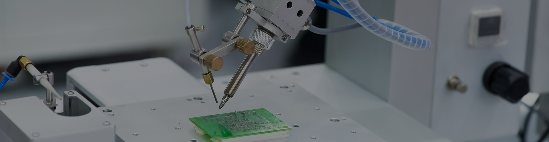
| flying probe tester PCB flying needle test machine is a kind of instrument for testing PCB board (printed circuit board) with high component layout, many layers, high wiring density and small measurement point distance, mainly testing the insulation and conduction value of the circuit board. The tester generally adopts the "truth value comparison positioning method", which can monitor the test process and fault point in real time to ensure the accuracy of the test. |

Line width and line distance tester The line width measuring instrument is mainly used to detect the upper and lower width and area, Angle, circle diameter, center distance of the line after the development and etching of the semi-finished product inside and outside the PCB printed circuit board. It can be extended to micro size measurement of other electronic components |
|

| Hole Check Hole inspection machine is mainly used for PCB drilling board and finished board drilling quality inspection and analysis. It can detect the defects of PCB drilling plate and finished plate such as few holes (missing drilling, plugging), porosity, burr in the hole, width of slot and other irregular hole shapes, and automatically determine the NG/OK classification equipment. |

ICT tester ICT,That is, automatic online testing, which is a necessary test equipment for modern PCB manufacturers, is very powerful. It is mainly through the test probe to contact the test point of the PCB layout to detect the PCBA line open circuit, short circuit, and fault of all parts, and clearly inform the staff. ICT has a wide range of use, high measurement accuracy, and clear indications of detected problems, making it easy for even workers with average electronic skills to deal with problematic PCBA. The use of ICT can greatly improve production efficiency and reduce production costs. |
|

PCBA Test Equipment
| SPI detection SPI(Solder paste detector) in the SMT patch processing is generally placed after the solder paste printing process, mainly used to detect the thickness of the solder paste on the circuit board, area, offset, etc., is an important equipment to monitor the solder paste printing quality. |

AOI detection AOI(The optical detector is placed in many places in the SMT factory, but it is generally placed behind the reflow welding in the actual processing, and is used to detect the welding quality of the reflow PCBA, so as to timely discover and eliminate defects such as less tin, less material, virtual welding, and tin |
|

| X-RAY detection X-RAY In fact, it is a common X-ray in hospitals, which uses high voltage impact on the target to produce X-ray penetration to detect the internal structural quality of electronic components, semiconductor packaging products, and SMT welding quality of various types of solder joints. X-RAY can detect all solder joints on the board, including those invisible to the naked eye, such as BGA. In addition, the defects that X-RAY detector can detect are mainly defects such as Bridges after welding, voids, welding joints that are too large, and welding joints that are too small. |

ICT detection ICT For production process control, it can measure resistance, capacitance, inductance and integrated circuit. It is especially effective for detecting open circuit, short circuit, component damage, etc., accurate fault location, easy maintenance. Can test after welding welding, open circuit, short circuit, component failure, wrong materials and other problems |
|

HL can provide you with high-quality SMT chip processing, SMT OEM service, one-stop PCBA processing, electronic OEM/ODM processing, Interli is committed to all the user value as the center, quality first, "quality" in the business philosophy, to the leading industry technology and international quality assurance system, to construct the technical core of their own, Produce high quality, high performance and the most competitive products, strive to build domestic and foreign brands, provide customers with quality service, strive to enhance customer value, create brilliant.
Our Newsletter
PCB
Assembly
Capabilities
About
Contact
- Building 18, Shayi North Yongfa Science Park, Xinhe
Road, Shajing Street, Bao'an District, Shenzhen, China
- Email:[email protected]
- Skype:
- WhatsApp:8613528898321
- Tel:+86 13528898321(David Wang )
- Fax:4007752975
Payment Methods:

Delivery Services

Verified by
