

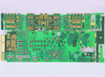
Multilayer pcb is a circuit board that has more than two layers.
unlike a double-sided pcb which only has two conductive layers of material, all multilayer pcbs must have at least three layers of conductive material which are buried in the center of the material.
How are multilayer pcbs made?
alternating layers of prepeg and core materials are laminated together under high temperature and pressure to produce multilayer pcbs. this process ensures that air isn’t trapped between layers, conductors are completely encapsulated by resin, and the adhesive that holds the layers together are properly melted and cured. the range of material combinations is extensive from basic epoxy glass to exotic ceramic or teflon materials.
Stack up for multilayer pcbs:
the following is the usual stackup information(4,6,8 layer pcb standard stackup), which also can be used as stackup of impedances.
in other special cases or advanced pcbs (you need to choose " additional options" and custom stackup or control impedance):
1. if you need custom stackup or control impedance, we will manufacture according to your requirement.
2. after place order,we will calculate whether it meets the requirements based on the stackup , material and impedance information.also we will confirm with you.
4-layer pcb standard stackup / 6-layer pcb standard stackup / 8-layer pcb standard stackup

the figure above illustrates the stackup of a 4-layer/ multilayer pcb. prepeg and core are essentially the same material, but prepeg is not fully cured, making it more malleable than the core.the alternating layers are then placed into a lamination press. extremely high temperatures and pressures are applied to the stackup, causing the prepeg to “melt” and join the layers together. after cooling off, the end result is a very hard and solid multilayer board.

Benefits of multilayer pcbs (compared to single or double-sided pcbs)
• higher assembly density
• smaller size (considerable savings on space)
• increased flexibility
• easier incorporation controlled impedance features.
• emi shielding through careful placement of power and ground layers.
• reduces the need for interconnection wiring harnesses (reduces overall weight)
Applications of multilayer pcbs
while the weight and space benefits of multilayer pcbs are especially valuable for aerospace pcbs, multilayer pcbs are also beneficial to applications where “cross-talk” levels are critical. these are a few other the applications using multilayer printed circuit boards:
| computers | file servers | data storage | signal transmission |
| cell phone transmission | cell phone repeaters | gps technology | industrial controls |
| satellite systems | hand held devices | test equipment | x-ray equipment |
| heart monitors | cat scan technology | atomic accelerators | central fire alarm systems |
| fiber optic receptors | nuclear detection systems | space probe equipment |

Honlynn is an experienced multilayer pcb manufacturer
honlynn circuit has been producing multilayer pcbs for over 12 years. over the years, we have seen all types of multilayer constructions from various industries, answered all types of multilayer questions, and solved all types of problems with multilayer pcbs.

Mass production lead time
| lead time Level | Lead Time (Wroking days,ex-factory | |
| Urgent(Days) | Normal(Days) | |
| 1、2L | 3-7 | 8-10 |
| 4L | 7-10 | 12-14 |
| 6、8L | 9-14 | 15-18 |
| 10L and up | To be determined based on case | |
The above lead time is based on:
1.Conventional Material
2.All engineering consultations is confirmed
 Online Support 24/7
24 hours fast PCB prototype expedite services
Free DFM & DFA Check
No minimum order requirement
Online Support 24/7
24 hours fast PCB prototype expedite services
Free DFM & DFA Check
No minimum order requirement
Our Newsletter
PCB
Assembly
Capabilities
About
Contact
- Building 18, Shayi North Yongfa Science Park, Xinhe
Road, Shajing Street, Bao'an District, Shenzhen, China
- Email:[email protected]
- Skype:
- WhatsApp:8613528898321
- Tel:+86 13528898321(David Wang )
- Fax:4007752975
Payment Methods:

Delivery Services

Verified by
