

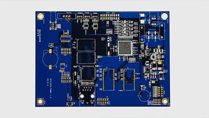
HDI PCB is the short form of high-density interconnect printed circuit board, a kind of printed circuit board manufacturing technology. An HDI PCB is a circuit board with a relatively high circuit density that uses micro-blind and buried “via”—or the copper-plated holes in PCBs—technology. HDI PCB are compact products designed for small-capacity users, as they cost much more than standard PCB.
HDI PCB boards, one of the fastest growing technologies in the PCB industry, are now available at HonLynn Circuit. HDI PCB contain both the blind via and buried via hole varieties and have a higher circuitry density than traditional circuit boards. We capable of manufacturing HDI PCB up to 36 layers.

HDI PCB stack-up suggestions
The following is a breakdown of the various structures offered by HonLynn:
1+N+1 – PCB contain 1 “build up” of high-density interconnection layers.
i+N+i (i≥2) – PCB contain 2 or more “build ups” of high-density interconnection layers. Microvias on different layers can be staggered or stacked.
Copper-filled stacked microvia structures are commonly seen in challenging designs.
4. Any Layer HDI – All the layers of a PCB are high-density interconnection layers, which allows the conductors on any layer of the PCB to be interconnected freely with copper-filled stacked microvia structures (“any layer via”). This provides a reliable interconnect solution for highly complex, large pin count devices, such as central processing unit (CPU) and graphics processing unit (GPU) chips utilized on handheld and mobile devices.
Honlynn HDI PCB capabilities
A microvia maintains a laser-drilled diameter of, typically, 0.006″ (150µm), 0.005″ (125µm), or 0.004″ (100µm), which are optically aligned and require a pad diameter of typically 0.012″ (300µm), 0.010″ (250µm), or 0.008″ (200µm), allowing additional routing density. Microvias can be via-in-pad, offset, staggered or stacked, non-conductive filled and copper-plated over the top, or solid copper filled or plated. Microvias add value when routing out of fine-pitch ball grid arrays (BGAs) such as 0.8 mm pitch devices and below.
| Step HDI | HDI Structures | Type of Micro vias | Mass Production | Small-Middle Batch | Prototype | Available |
| 1+N+1 | Blind vias | Yes | Yes | Yes | 4 Layers+ | |
| 2 Step | 2+N+2 | Blind/Buried staggered vias | Yes | Yes | Yes | 6 Layers+ |
| 2 Step | 2+N+2 | Blind/Buried stacked vias | Yes | Yes | Yes | 6 Layers+ |
| 3 Step | 3+N+3 | Blind/Buried staggered vias | Yes | Yes | Yes | 8 Layers+ |
| 3 Step | 3+N+3 | Blind/Buried stacked vias | Yes | Yes | Yes | 8 Layers+ |
| 4 Step | 4+N+4 | Blind/Buried Vias | Yes | Yes | Yes | 10Layers+ |
| 5 Step | 5+N+5 | Blind/Buried Vias | Yes | Yes | Yes | 12 Layers+ |
Additionally, microvias add value when routing out of a 0.5 mm pitch device where staggered microvias can be used. However, routing micro-BGAs such as a 0.4 mm, 0.3 mm, or 0.25 mm pitch device, requires the use of Stacked MicroVias using an inverted pyramid routing technique.
HonLynn capable of manufacturing HDI PCB up to 36 layers
Conclusion
We hope we were able to answer all your questions regarding HDI PCBs. When choosing an HDI PCB, please make sure you check the specifications. These specifications include materials used and your HDI PCB design.
HDI PCB material
Some new requirements are being put forward for HDI PCB materials, including better dimensional stability, antistatic mobility, and non-adhesives. The typical material of HDI PCBs is Resin-Coated-Copper (RCC). There are three types of RCCs—namely, polyimide metallized film, pure polyimide film, and cast polyimide film.
The advantages of RCCs include: small thickness, light weight, flexibility and reduced flammability, compatibility characteristic impedance, and excellent dimensional stability. In the HDI multi-layer PCB process, instead of the traditional adhesive sheet and copper foil as the insulating medium and conductive layer, the RCC can be suppressed with the chip using traditional suppression technology. Non-mechanical drilling methods such as lasers are then used to form microvia interconnections.
RCC promotes the development of PCB products from surface mount technology (SMT) to chip-scale packaging (CSP), from mechanical drilling to laser drilling—and promotes the development and progress of PCB microvias, all of which have become RCC’s leading HDI PCB material.
In the actual PCB manufacturing process, for the selection of RCC, there are usually FR-4 standard Tg 140C, FR-4 high Tg 170C, and FR-4 and Rogers combined lamination, which are mostly used now. Given the development of HDI technology, HDI PCB materials must meet more requirements. Therefore, the main trends of HDI PCB materials are:
1. Development and application of flexible materials without adhesives;
2. The thickness of the dielectric layer is small and the deviation is small;
3. The development of LPIC;
4. The dielectric constant is getting smaller and smaller;
5. The dielectric loss is getting smaller and smaller;
6. High welding stability; and
7. Strictly compatible with coefficient of thermal expansion (CTE).
HDI PCB advantages
1. HDI technology can reduce the cost of PCB, although when the density of PCB increases beyond eight layers, it will be more expensive to manufacture with HDI.
2. The traditional and complex pressing process is low.
3. Increased circuit density: traditional circuit boards and parts are interconnected
4. Conducive to the use of advanced construction technology
5. Have better electrical performance and signal accuracy
6. Better reliability
7. Can improve thermal properties
8. Can improve radio frequency interference/electromagnetic wave interference/electrostatic discharge (RFI/EMI/ESD)
9. Greater design efficiency
HDI PCB application

6 layer Blind via hole HDI PCB
While advancements in electronic design continue to improve the performance of the whole device, the trend is also moving towards reducing its size. In small portable products ranging from mobile phones to smart weapons, “small” is an eternal pursuit. High-density interconnect (HDI) technology can make terminal product designs more compact, while meeting higher standards of electronic performance and efficiency. HDIs are widely used in mobile phones, digital cameras, MP3s, MP4s, notebook computers, automotive electronics ,and other digital products, among which mobile phones are the most widely used. HDI boards are generally manufactured by the build-up method.
The greater the build-up times, the higher the technical level of the board. Ordinary HDI boards are basically one-time build-up. High-end HDIs use two-time, or more, build-up technology. At the same time, advanced PCB technologies such as stacking holes, electroplated hole filling, and laser direct drilling are used. High-end HDI PCB boards are mainly used in 3G, 4G, and 5G mobile phones, advanced digital cameras, IC carrier boards, etc.
Assuming the upward trend of high-end HDI PCB boards, 4G boards, or IC carrier boards continues, future growth is expected to be very rapid: the world’s 5G mobile phone use will grow by more than 50% in the next few years, and China will issue 5G licenses. Moreover, IC carrier board industry consulting agency Prismark predicts that China’s forecast growth rate from 2020 to 2030 will be 80%, which is microcosmic of the direction of PCB technology development.
HDI PCB manufacturing technology

8 layer Hdi PCB
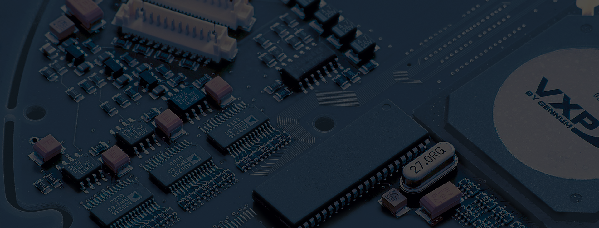
The difficulty in HDI PCB manufacturing is microvias, which are made through metallization and thin wires.
1. Microvia manufacturing
Microvia manufacturing has always been the core issue of HDI PCB manufacturing. There are two main drilling methods:
1.Mechanical drilling, which for ordinary through hole drilling is always the best choice for its high efficiency and low cost. With the development of machining capabilities, its application in microvias is also constantly developing.
2.Laser drilling, of which there are two types: photothermal ablation and photochemical ablation. The former refers to a process by which the operating material is heated to melt and evaporate through the formed through hole after the high-energy laser is absorbed. The latter refers to the result of high-energy photons and lasers exceeding 400nm in the ultraviolet region.
There are three types of laser systems applied to flexible and rigid boards, namely excimer lasers, ultraviolet laser drilling, and CO2 lasers. Laser technology is not only suitable for drilling, but also for cutting and forming. Some manufacturers even use lasers to manufacture HDIs.
Although the cost of laser drilling equipment is high, they have higher precision as well as stable and mature technology. The advantages of laser technology make it the most commonly used method in blind/buried through hole manufacturing. Today, 99% of HDI microvias are obtained by laser drilling.
2. Through metallization
The biggest challenge of through-hole metallization is that it is difficult to achieve uniform plating. For the deep-hole electroplating technology of microvias, in addition to the use of an electroplating solution with high dispersibility, the plating solution on the electroplating device should be upgraded in time. This can be done through strong mechanical stirring or vibration, ultrasonic stirring, and horizontal spraying. In addition, the humidity of the through-hole wall must be increased before plating.
In addition to process improvements, HDIs’ through-hole metallization method has also seen major technological improvements: these include chemical plating additive technology, direct electroplating technology, etc.
3rd. Tiny circuit
The realization of thin lines includes traditional image transmission and direct laser imaging. Traditional image transfer is the same as the process of forming lines by ordinary chemical etching.
For direct laser imaging, no photographic film is needed, and the image is formed directly on the photosensitive film by laser. The ultraviolet (UV) lamp is used for operation, so that the liquid anticorrosion solution can meet the requirements of high resolution and simple operation. No photographic film is needed to avoid adverse effects associated with film. CAD/CAM can be directly connected to shorten the manufacturing cycle and make it suitable for limited and multiple production.
Tips: How the name “HDI” originated
HDI stands for high-density interconnect, a type of manufacturing printed circuit board (PCB). The PCB is a structural element formed by insulating materials and conductor wiring. When printed circuit boards are assembled into final products, integrated circuits, transistors (transistors, diodes), passive components (such as resistors, capacitors, connectors, etc.) and various other electronic parts are mounted on them.
With the help of wire connection, it is possible to form an electronic signal connection and function. Therefore, PCB is a platform that provides component connection and is used to accept the substrate of the connected parts.
Since the printed circuit board is not a general terminal product, the definition of the name is slightly confusing. For example, the motherboard for personal computers is called the motherboard and cannot be directly called the circuit board. So, when evaluating the industry, the two are related but not the same. Another example: because there are integrated circuit components mounted on the circuit board, the news media calls it an integrated circuit board (IC board), but in essence it is not equivalent to a printed circuit board.
Given the premise that electronic products tend to be multi-functional and complex, the contact distance of integrated circuit components has been reduced, and the speed of signal transmission has been relatively increased. This is followed by an increase in the amount of wiring and the local length of wiring between points. In short, these require the application of high-density circuit configuration and microvia technology to achieve the goal.
Wiring and jumpers are difficult to achieve for single and double panels, so the circuit board will be multi-layered—and because of the continuous increase of signal lines, more power layers and grounding layers are a necessary means for design. All of these have made multilayer PCBs more common.
For the electrical requirements of high-speed signals, the circuit board must provide impedance control with alternating current characteristics and high-frequency transmission capabilities, and it also must reduce unnecessary radiation (EMI). Given the structure of striplines and microstrips, multilayer design becomes a necessity. In order to reduce the quality of signal transmission, insulating materials with low dielectric coefficients and low attenuation rates are used.
In order to match the miniaturization and arraying of electronic components, the density of circuit boards is continuously increased to meet demand. The emergence of assembly methods such as ball grid arrays (BGAs), chip scale packages (CSPs), and direct chip attachment (DCAs) has promoted printed circuit boards to an unprecedented high-density state.
Any hole with a diameter of less than 150um is called a microvia in the industry. The circuit made by the geometric structure technology of this microvia can improve the efficiency of assembly, space utilization, etc., and it is also useful for the miniaturization of electronic products. It is a necessity.
For circuit board products of this structure, the electronics industry has had many different names for PCBs. For example, because European and American companies used the sequential construction method to produce the program, they called this type of product SBU (Sequence Build Up Process). As for Japanese companies, because the pore structure produced by this type of product is much smaller than that of the previous pores, the production technology of this type of product is called MVP (Micro Via Process), which is generally translated as “Micro Via Process.”
Some people call this type of circuit board BUM (Build Up Multilayer Board) because the traditional multi-layer board is called MLB (Multilayer Board), which is generally translated as “build-up multilayer board.”
In the interest of avoiding confusion, the IPC Circuit Board Association of the United States proposed to call this kind of product technology the common name of HDI—or, high-density interconnect technology. If it is directly translated, it becomes a high-density interconnection technology. However, this does not reflect the characteristics of the circuit board, so most circuit board manufacturers call this type of product an HDI board, or the full Chinese name “High Density Interconnection Technology.” However, because of the quirks of spoken language, some people directly call it a “high-density circuit board” or HDI PCB board.
HDI PCB: types
HDI PCB comes in different types. Although they are different, with respect to designs, they have the same function. The type you decide to choose depends on the application you are using. Let’s quickly consider the types.
* Flex HDI PCB
Flex HDI PCB is composed of flexible plastic. This material permits the board to form different shapes. This offers lots of benefits when compared with rigid boards.
The board’s flexibility also allows you to move or bend easily during the process of application without bringing damage to the circuits that are present on the board. One disadvantage with this board type is that designing and manufacturing it costs a lot. However, they come with numerous benefits.
The heavy wiring found in advanced equipment like satellites can be replaced with these PCBs. They are lighter and make use of little space, making them great for such use. Another benefit is that it features different designs like multilayer, single-sided, or double-sided designs.
* Rigid HDI PCB
Asides the number of layers and sides that this HDI PCB has, it also comes in different rigidities. They are made up of a solid and rigid substrate material such as fiberglass. This kind of material prevents the bending of the HDI board. The application of this HDI PCB can be found on towers of most desktops.
* Rigid-Flex HDI PCB
This is made up of a rigid circuit board, which attaches to a flexible board. The design’s complexity depends on whatever application you are using.
* Multilayer HDI PCB
These boards have substrate boards of multiple layers with an insulating material that separates these layers. Just like HDI PCBs with double sides, either vias or through holes can be used in connecting the board’s electric circuits. Multilayer HDI PCBs are very beneficial because they use less space. Standard applications using this HDI board type include medical machinery, servers, handheld devices, and computers.
Mass production lead time
| lead time Level | Lead Time (Wroking days,ex-factory | |
| Urgent(hours) | Normal(days) | |
| 1+N+1 | 10-12 | 15-18 |
| 2+N+2 | 18-22 | 18-22 |
| 3+N+3 | 22-24 | 22-24 |
| 4+N+4 | To be determined based on case | |
The above lead time is based on:
1.Conventional Material
2.All engineering consultations is confirmed
 Online Support 24/7
24 hours fast PCB prototype expedite services
Free DFM & DFA Check
No minimum order requirement
Online Support 24/7
24 hours fast PCB prototype expedite services
Free DFM & DFA Check
No minimum order requirement
Our Newsletter
PCB
Assembly
Capabilities
About
Contact
- Building 18, Shayi North Yongfa Science Park, Xinhe
Road, Shajing Street, Bao'an District, Shenzhen, China
- Email:[email protected]
- Skype:
- WhatsApp:8613528898321
- Tel:+86 13528898321(David Wang )
- Fax:4007752975
Payment Methods:

Delivery Services

Verified by
