

Why design heavy copper PCB (extreme copper PCB)?
HonLynn provide extreme copper PCB manufacturing service, Outlayer Max up to 20oz, Inner max to 10 Oz, Send your PCB Files to [email protected] , Get a Quote Now !

The heat sinking capacity of Heavy Copper PCBs is much higher as compared to casual PCBs. Heat sinking is vitally essential for the development of a robust and durable circuit. Poor handling of heat signals not only affects electronics performance but also shortens the life of circuitry.
HonLynn support 10 OZ Inner layer , 20 OZ Out layer Extreme copper pcb manufacturing, Send your pcb file to get quote now.

8 Layer PCB Inner 8oz, 20 oz Out layer
As the electronic industry evolves, the demand for heavy copper PCB continues to increase. Printed circuit boards are the heart of the electronic industry. These boards play a vital role in the production of electronics. Heavy copper PCB is the most recent trend in the PCB industry.
This type of PCB offers some features and benefits. Heavy copper PCB is useful in several applications due to its properties. In this article, we will tell you everything you need to know about this type of PCB.
What is heavy copper PCB?
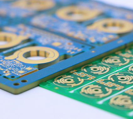
Heavy copper PCB is a circuit board with a copper thickness that is ≥ 3oz per sq. ft in its outer and inner layers. What makes a circuit board classified as a heavy copper PCB is its thicker plating. During the production of heavy copper PCB, copper thickness is enhanced through plated holes and sidewalls.
For instance, when a PCB has 2 ounces of copper per sq. ft thickness, it is a standard PCB. However, if it has more than 3oz of copper, it is a heavy copper PCB. Heavy copper PCB is considered a reliable wiring option. Heavy copper PCB is different from extreme copper PCB which features within 20 oz to 200 oz per sq. ft.
The extra copper thickness allows the board to conduct more current. Heavy copper PCB has strong mechanical power in the plated-through-holes and connector sites. This type of PCB is also known as thick copper PCB.
What does heavy copper PCB offer?
Heavy copper PCB has a lot to offer. It has got some unique features that make it an ideal option for high-end applications. Let’s discuss some of the benefits of this PCB;
Great thermal distribution: Due to its copper-plated vias, this PCB offers high thermal resistance. Heavy copper PCB are used in applications that demand high speed and high frequency. You can also use this PCB at harsh temperatures.
Mechanical strength: Heavy copper PCB feature great mechanical strength. When this PCB is used, it makes the electrical system durable and robust.
Good conductor: Heavy copper circuit boards are a good conductor. They are utilized in the production of electronics due to this feature. They help to link various boards together. These boards can transfer current.
Onboard heat sink: Heavy copper boards offer an onboard heat sink. With these boards, you can achieve effective heat sinks on mosaic surfaces.
Great dissipation factor: Heavy copper PCB are ideal for large components with a high loss of power. These PCBs prevent overheating from occurring in electrical systems. They dissipate excess heat effectively.
Supports exotic material: Heavy copper helps to protect and enhance exotic material. Exotic materials are sometimes used for designing electronic components. An extreme temperature may need an exotic material. Heavy copper boards end circuit failures because they use an exotic material to its full capabilities.
How is heavy copper PCB fabricated?
For the fabrication of heavy copper PCB, plating or etching is often used. The main aim is to add copper thickness to sidewalls and plated holes. The methods used in fabricating heavy copper PCB aren’t far-fetched. Heavy copper PCBs need special etching and plating methods to ensure the extra thickness of copper.
Using the normal etching techniques for the fabrication of heavy copper PCBs isn’t ideal. Normal etching methods produce over-etched margins and edge lines that are uneven. PCB producers now use advanced etching and plating methods to achieve straight edges.
During the PCB fabrication process, heavy copper PCBs are electroplated. This will help thicken the walls of PTH on the PCB. With this technique, the layer count shrinks and the impedance distribution reduces. When PCBs are exposed to several cycles during the manufacturing process, the plated holes can become weak.
The fabrication of heavy copper PCBs has its limitations which include;
· The etching process increases the cost
· The etching process requires a huge amount of copper to be removed
· It is hard to fabricate finer lines and thick copper traces
· Heavy copper traces make the surface uneven
Methods for fabricating heavy PCBs
Manufacturers utilize different techniques for fabricating heavy copper PCBs.
Embedded copper method: This method fabricates heavy copper PCB using a flat surface. Here the heavy copper is inserted within the prepreg resin. The thickness of the resin determines the thickness of the copper.
For instance, the fabricator begins with a 6-mil laminate and a 1 0z copper clad. Then the copper clad is covered with a photoresist. After this, a 5-mil laser beam is used to cut the circuit pattern from the side of the laminate. The laser has to cut via the laminate to the copper foil. If the laser is controlled, the fabricator can prevent the copper foil from damage.
The fabricator positions the laminate into a plating tank to electroplate. The copper plating produces about 6 mil plating thickness after filling the laser cut groove on the laminate.
Blue bar method: The blue bar method involves inserting thick copper bars into circuit boards. This method saves the material and reduces the weight of the PCB. During the fabrication process, the resin flows into space within the copper traces, this helps to achieve an even top surface.
Fabricators must pay attention to the level of copper fill between inner layers when it comes to multilayer boards with heavy copper layers. Low levels of fill and low levels of resin can lead to resin hunger.
Heavy copper PCB capabilities
It is important to consider the capabilities of heavy copper PCB when using them for some applications. This type of PCB is more expensive to produce based on their requirements. A heavy copper PCB should have these capabilities;
· A minimum board size of 6mm by 6mm and a maximum board size of 457mm by 610mm
· Copper thickness is greater than 3oz for each square foot.
· A board thickness between 0.6mm and 6mm
· Maximum external layer copper weight should be 15oz
· Solder mask color should be either green, blue, red, black, white, purple, or yellow
· Silkscreen color is white, yellow, or black
· The surface finishing should be Immersion Gold, OSP, and HASL
· The finished thickness is between 0.020 inches and 0.275 inches
Difference between a standard PCB and thick copper PCB
Standard PCBs can be produced with copper etching and plating processes. These PCBs are plated to add copper thickness to planes, traces, PTHs, and pads. The amount of copper used in the production of standard PCBs is 1oz. In the production of heavy copper PCB, the amount of copper used is greater than 3oz.
For standard circuit boards, copper etching and plating techniques are utilized. However, heavy copper PCBs are produced via differential etching and step platting. Standard PCBs perform lighter activities while heavy copper boards perform heavy duties.
Standard PCBs conduct lower current while heavy copper PCBs conduct higher current. Thick copper PCBs are ideal for high-end applications due to their efficient thermal distribution. Heavy copper PCBs have better mechanical strength than standard PCBs. Heavy copper circuit boards enhance the capability of the board in which they are utilized.
Other features that make thick copper PCBs different from other PCBs
Copper weight: This is the main distinguishing feature of heavy copper PCBs. Copper weight refers to the weight of the copper used in a square foot area. This weight is usually measured in ounces. It indicates the copper’s thickness on the layer.
Outer layers: These refer to the external copper layers of the board. Electronic components are usually bonded to the external layers. The external layers begin with copper foil which is coated with copper. This helps to increase the thickness. The copper weight of the external layers is preset for standard designs. Heavy copper PCB manufacturer can alter the weight and thickness of the copper to suit your requirement.
Inner layers: The dielectric thickness, as well as the copper mass of the internal layers, is predefined for the standard projects. However, the copper weight and thickness in these layers can be adjusted based on your needs.
Applications of heavy copper PCB
Heavy copper PCB offers some outstanding features that make it ideal for certain applications. This type of PCB is used in military and defense applications. The demand for heavy copper PCBs has been increasing over the years. This is because these PCBs are used in several applications such as;
· Rail traction systems
· UPS systems
· Solar power converters
· Nuclear power industries
· Automotive industries
· Torque controls
· Power line motors
· Welding equipment
· Military equipment
· Safety and signal systems
· Protection relays
Conclusion
Heavy copper PCBs are produced via etching and plating methods. The major aim in the production of this PCB is to add copper thickness through sidewalls and plated-through holes. Heavy copper PCBs have several benefits which make them in high demand.
Due to their outstanding features and benefits, they can meet your electrical requirements. These circuit boards will always dissipate heat generated due to heavy currents conduction. Electronics using heavy copper boards have been in use for a long time. Heavy copper can carry high currents. These boards will continue to meet the needs of various applications.
High power circuit wirings can be developed using Heavy Copper PCBs. Such a wiring mechanism offers more reliable thermal stress handling and offers fine finishing while incorporating multiple channels on a single layer of a compact board.
Heavy Copper PCBs are widely used in various products as they provide multiple features for improving circuit performance. These PCBs are widely used in high power equipment such as transformers, heat sinking, power inverters, military equipment, solar panels, automotive products, welding plants, and power distribution systems.
Heavy Copper PCB generally need to adopt a special pressing procedure. It involves the use of multiple PP fillings to meet the required filling during the pressing process. The pressing involves high pressure and a large flow of glue. There are empty areas in the heavy copper PCB in each layer of the inner layer pattern; there is no copper in the open area. Also, the edge of the plate is designed with a single air guide groove.
Due to the high pressure, the amount of PP glue passes very easily, and the air guide grooves are lost. This causes the thickness of the board in the open area to be too thin. The board’s overall thickness is extremely large, which causes the film to be not tight during the subsequent processing of the outer layer, ultimately causes the product to be not useable.
The priority is to reduce the flow of glue in the open area and prevent the open area’s thickness from being too thin. This is an urgent problem to be solved in the production process for such heavy copper PCB .
How to solve issue of the uniform thickness in the production of heavy coppy PCB
1.This is amethod for manufacturing a heavy copper PCB with uniform thickness. Each inner core plate of the heavy copper PCB is provided with a copper-free open area at the same position, which includes the following steps:
· Cut the material to obtain the inner core board. Through the inner layer pattern and etching process, the inner layer lines are made on each inner core board, and some copper PADs are staggered on the edge of the open area of each inner core board. Made each inner layer board.
· The inner layer board and the outer layer copper foil are pressed together by the prepreg to make a multi-layer production board.
· Post-processing the multi-layer production board according to the existing technology to obtain a thick copper board.
2.The method for manufacturing a heavy copper PCB with uniform thickness according to claim 1, wherein the copper PAD in step S1 has the same shape and size, all of which are round, oval, diamond, or square.
3.This is a method for manufacturing thick copper plates with uniform thickness according to claim 2. The radius of each copper PAD is R, and at least two rows of circular shapes are provided on the edge of the open area of the inner core plate. The copper PADs in each row are arranged equidistantly along the long edge of the board. The center distance between two adjacent copper PADs is any two adjacent copper PADs in each row.
The bottom copper PAD is called the bottom copper PAD. The copper PAD between the bottom copper PAD is the corresponding vertex copper PAD. The center of each bottom copper PAD and the corresponding vertex copper PAD are connected to form an isosceles right triangle.
4.A thick copper plate with uniform thickness is comprised of at least one inner layer core plate. Each inner layer core plate is provided with a copper-free open area and at the same position, characterized in the open area of the inner layer core plate. Several copper PADs are staggered on the edge of the board.
5.The heavy copper PCB with uniform thickness according to claim 4, wherein the shape of the copper PAD is a circle, an oval, a diamond, or a square.
6.The heavy copper PCB with uniform thickness according to 5, each copper PAD has a radius R, and at least two rows of circular copper PAD are provided on the edge of the inner core plate’s open area. The copper PADs in each row are arranged equidistantly along the long edge of the board. The center distance between two adjacent copper PADs is any two adjacent copper PADs in each row;
they are called bottom copper PADs. Adjacent rows are located on the bottom side. The copper PAD between the copper PADs is the corresponding vertex copper PAD. The center of the two base copper PADs and the corresponding vertex copper PAD centers form an isosceles right triangle.
Mass production lead time
| lead time Level | Lead Time (Wroking days,ex-factory | |
| Urgent(days) | Normal(days) | |
| 1、2L | 4-8 | 9-11 |
| 4L | 8-11 | 13-15 |
| 6、8L | 10-15 | 16-18 |
| 10L and up | To be determined based on case | |
The above lead time is based on:
1.Conventional Material
2.All engineering consultations is confirmed
 Online Support 24/7
24 hours fast PCB prototype expedite services
Free DFM & DFA Check
No minimum order requirement
Online Support 24/7
24 hours fast PCB prototype expedite services
Free DFM & DFA Check
No minimum order requirement
Our Newsletter
PCB
Assembly
Capabilities
About
Contact
- Building 18, Shayi North Yongfa Science Park, Xinhe
Road, Shajing Street, Bao'an District, Shenzhen, China
- Email:[email protected]
- Skype:
- WhatsApp:8613528898321
- Tel:+86 13528898321(David Wang )
- Fax:4007752975
Payment Methods:

Delivery Services

Verified by
