
Today, the editor of Honglian Circuit will take you to see how a PCB board was born. Firstly, how was a PCB born? Before the emergence of a PCB, the circuit was composed of point-to-point wiring. The reliability of this method is very low because as the circuit ages, the rupture of the circuit can lead to an open circuit or short circuit at the circuit nodes. Wire winding technology is a significant advancement in circuit technology, which improves the durability and replaceability of circuits by wrapping small diameter wires around pillars at connection points. As the electronics industry evolves from vacuum tubes and relays to silicon semiconductors and integrated circuits, the size and price of electronic components are also decreasing. Electronic products are increasingly appearing in the consumer field, prompting manufacturers to search for smaller and more cost-effective solutions. So, PCB was born.
PCB layout
The first step in PCB production is to organize and check the PCB layout. The PCB manufacturing factory receives CAD files from the PCB design company. As each CAD software has its own unique file format, the PCB factory will convert them to a unified format - Extended Gerber RS-274X or Gerber X2. Then the factory engineers will check whether the PCB layout conforms to the manufacturing process and whether there are any defects or other issues.
Production of core board
Clean the copper clad plate. If there is dust, it may cause the final circuit to short or open.
The following figure is the legend of an 8-layer PCB, which is actually composed of 3 copper clad boards (core boards) and 2 copper films, and then glued together with semi cured sheets. The production sequence starts from the middle core board (4, 5 layers of circuits), continuously stacking them together, and then fixing them. The production of a 4-layer PCB is also similar, except that only one core board and two copper films are used.
Inner PCB layout
To transfer the layout of the inner layer PCB, the first step is to create the two layers of circuits for the middle core board. After cleaning the copper clad plate, a layer of photosensitive film will be covered on the surface. This film will solidify when exposed to light, forming a protective film on the copper foil of the copper clad plate.
Insert two layers of PCB layout film and double layer copper clad plate, and finally insert the upper layer of PCB layout film to ensure accurate stacking position of the upper and lower layers of PCB layout film.
The photosensitive machine uses a UV lamp to illuminate the photosensitive film on copper foil. Under the transparent film, the photosensitive film is cured, while under the opaque film, there is still no cured photosensitive film. The copper foil covered under the solidified photosensitive film is the required PCB layout circuit, equivalent to the function of laser printer ink for manual PCBs.
Then clean the uncured photosensitive film with alkaline solution, and the required copper foil circuit will be covered by the cured photosensitive film.
Then use strong alkali, such as NaOH, to etch off the unnecessary copper foil.
Tear off the cured photosensitive film and expose the required PCB layout copper foil.
Core plate punching and inspection
The core board has been successfully manufactured. Then make alignment holes on the core board for easy alignment with other raw materials. Once the core board is pressed together with other layers of PCBs, it cannot be modified, so inspection is very important. The machine will automatically compare with the PCB layout drawings to check for errors.
Lamination
A new raw material called semi cured sheet is needed here, which is the adhesive between the core board and the core board (with PCB layers>4), as well as between the core board and the outer copper foil, and also serves as insulation.
The lower layer of copper foil and two layers of semi cured sheet have been fixed in place through alignment holes and the lower layer of iron plate in advance. Then, the prepared core plate is also placed into the alignment holes, and finally, two layers of semi cured sheet, one layer of copper foil, and one layer of pressure bearing aluminum plate are covered on the core plate in sequence.
Place the PCB boards clamped by the iron plate on the bracket and then send them into a vacuum hot press for lamination. The high temperature in the vacuum hot press can melt the epoxy resin in the semi cured sheet, fixing the core plates and copper foil together under pressure.
After the lamination is completed, remove the upper iron plate that presses the PCB. Then remove the pressure bearing aluminum plate, which also serves to isolate different PCBs and ensure the smoothness of the outer copper foil of the PCB. At this point, both sides of the PCB that is taken out will be covered with a smooth layer of copper foil.
drill hole
To connect the four layers of non-contact copper foil in a PCB together, first drill through holes that run through the PCB from top to bottom, and then metallize the hole walls to conduct electricity.
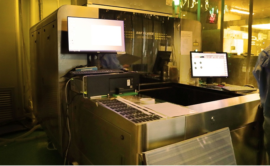
Use an X-ray drilling machine to position the inner core board. The machine will automatically find and locate the hole position on the core board, and then drill a positioning hole on the PCB to ensure that the next drilling passes through the center of the hole position.
Place a layer of aluminum plate on the punching machine tool, and then place the PCB on top. In order to improve efficiency, 1-3 identical PCB boards will be stacked together for perforation based on the number of layers of the PCB. Finally, cover the top PCB with a layer of aluminum plate. The upper and lower layers of aluminum plate are designed to prevent tearing of the copper foil on the PCB when the drill bit drills in and out.
In the previous lamination process, the melted epoxy resin was squeezed onto the outside of the PCB, so it needs to be cut off. The profiling milling machine cuts the periphery of the PCB according to its correct XY coordinates.
Copper chemical precipitation on the pore wall
Due to almost all PCB designs using perforations to connect different layers of circuits, a good connection requires a 25 micron copper film on the hole wall. This thickness of copper film needs to be achieved through electroplating, but the hole wall is composed of non-conductive epoxy resin and fiberglass board.
So the first step is to first stack a layer of conductive material on the hole wall, and form a 1-micron copper film on the entire PCB surface, including the hole wall, through chemical deposition. The entire process, such as chemical treatment and cleaning, is controlled by machines.
Fixed PCB
Clean PCB
Shipping PCB
Transfer of outer PCB layout
Next, the outer layer PCB layout will be transferred to copper foil, and the process is similar to the previous inner layer core board PCB layout transfer principle. Both use photocopying film and photosensitive film to transfer the PCB layout to copper foil, with the only difference being that the positive film will be used as the board.
The transfer of the inner PCB layout adopts the subtraction method, which uses a negative film as the board. The PCB is covered by a cured photosensitive film, and the uncured photosensitive film is cleaned. After the exposed copper foil is etched, the PCB layout circuit is protected by the cured photosensitive film and left behind.
The outer PCB layout transfer adopts the normal method, using positive chips as the board. The non circuit area is covered by the cured photosensitive film on the PCB. Clean the uncured photosensitive film before electroplating. Where there is a film, electroplating is not possible, but where there is no film, copper should be plated first and then tin. After removing the film, perform alkaline etching and finally remove the tin. The circuit diagram is left on the board due to the protection of tin.
Clamp the PCB with a clip and electroplate the copper onto it. As mentioned earlier, in order to ensure sufficient conductivity at the hole site, the copper film electroplated on the hole wall must have a thickness of 25 microns. Therefore, the entire system will be automatically controlled by a computer to ensure its accuracy.
Outer PCB etching
Next, a complete automated assembly line will complete the etching process. Firstly, clean the cured photosensitive film on the PCB board. Then use strong alkali to clean the unnecessary copper foil covered by it. Remove the tin coating from the PCB layout copper foil using a tin removal solution. After cleaning, the 4-layer PCB layout is completed.
These processes are fundamental for PCB manufacturers. Macro connected circuit 4-layer PCB professional circuit boards are produced in small and large quantities, serving over 10000 customers. We are professional in producing PCBs, and we are also the preferred supplier for special processes such as impedance boards, halogen-free boards, half hole boards, high TG boards, high-frequency boards, tin silver copper, thick copper boards, etc. If you are interested, please contact us at 400-775-2975
Popular Blog Posts

PCB Manufacturing & Assembly Service
 File Upload


Our Newsletter
PCB
Assembly
Capabilities
About
Contact
- Building 18, Shayi North Yongfa Science Park, Xinhe
Road, Shajing Street, Bao'an District, Shenzhen, China
- Email:[email protected]
- Skype:
- WhatsApp:8613528898321
- Tel:+86 13528898321(David Wang )
- Fax:4007752975
Payment Methods:

Delivery Services

Verified by
