

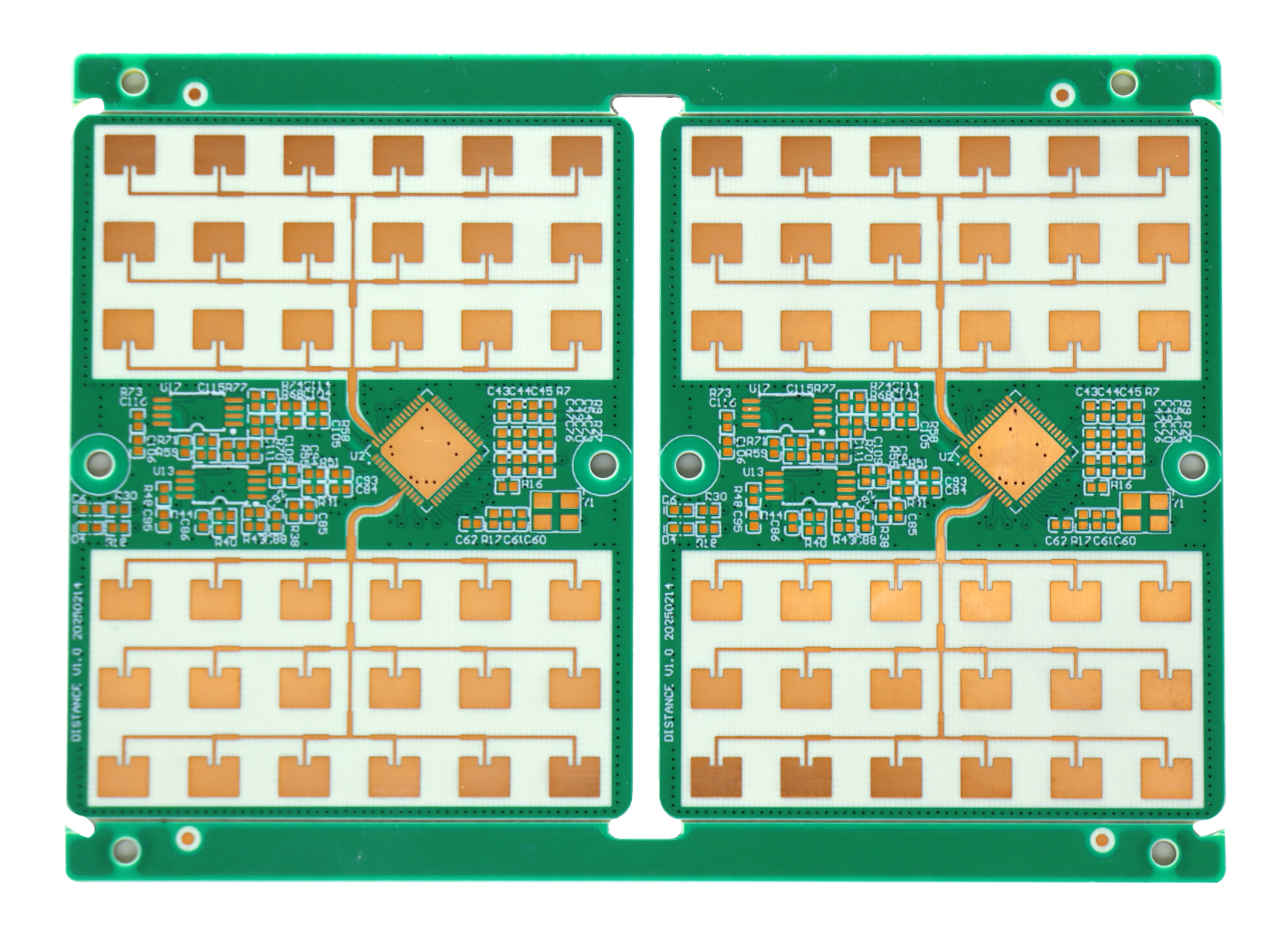

Key technologies and materials for high-frequency and high-speed PCBs
1. Core materials
This is the fundamental difference from ordinary PCBs.
Low-loss board:
Characteristics: It possesses a **low and stable dielectric constant and an extremely low dielectric loss factor.
Common brands include Rogers, Taconic, Isola, and the Megtron series from Panasonic.
Compared to FR-4: FR-4 has an unstable Dk value and a high Df value, making it unsuitable for high-frequency and high-speed applications.
2. Design and wiring technology
Transmission line theory: It is necessary to use controllable impedance transmission lines, such as microstrip lines and striplines, and accurately calculate their geometric dimensions to achieve the target impedance.
Strict layered design: Provides a clear signal return path, reduces loop area, and controls impedance. Multiple ground layers and power layers are typically used.
Differential pair routing: For high-speed serial signals (such as PCIe, USB, SATA), it is necessary to use equal-length, equally-spaced, and symmetrical differential pair routing to enhance anti-interference capability.
Via optimization: Vias are the main source of impedance discontinuity. It is necessary to use back drilling to remove useless via stubs, or use blind buried via technology to reduce the impact of vias on the signal path.
Main application areas
Communication equipment: 5G base stations/antennas, optical transmission network equipment, microwave relay equipment.
Data center and computing: high-end servers, routers, switches, AI accelerator cards.
Automotive electronics: millimeter-wave radar, in-vehicle infotainment systems, advanced driver assistance systems.
Aviation, Aerospace, and Defense: Radar Systems, Satellite Communications, Electronic Warfare Equipment.
High-end testing instruments: network analyzer, high-speed oscilloscope.

Prototype sample lead time
| lead time Level | Lead Time (Wroking days,ex-factory) | |
| Urgent(hours) | Normal(days) | |
| 1、2L | 24 | 3-4 |
| 4L | 48 | 7-8 |
| 6、8L | 72 | 7-10 |
| 10L and up | To be determined based on case | |
The above lead time is based on:
1.Conventional Material
2.All engineering consultations is confirmed
 Online Support 24/7
24 hours fast PCB prototype expedite services
Free DFM & DFA Check
No minimum order requirement
Online Support 24/7
24 hours fast PCB prototype expedite services
Free DFM & DFA Check
No minimum order requirement
Our Newsletter
PCB
Assembly
Capabilities
About
Contact
- Building 18, Shayi North Yongfa Science Park, Xinhe
Road, Shajing Street, Bao'an District, Shenzhen, China
- Email:[email protected]
- Skype:
- WhatsApp:8613528898321
- Tel:+86 13528898321(David Wang )
- Fax:4007752975
Payment Methods:

Delivery Services

Verified by
